CKQ7K325T
CLBs
6 Input Lookup Table (LUT)
Features with storage logic
It has the function of registers and shift registers
CMT
High-rate caching and low-jitter clock cabling schemes
Frequency synthesis and phase shifting
Low-jitter clock generation and jitter filtering
DSP Slice
25 x 18 bit multiplier and accumulator with complement function
Low-power pre-adders - selectable pipelining, ALU, and cascading
Block RAM
Dual-port 36Kb RAM block with up to 72-bit bit width - built-in FIFO logic
Built-in selectable error correction circuit
Select IO interface technology
High-performance Select IO technology with DDR3 interface support
High-frequency decoupling capacitors can improve package integration
Numerically controlled impedance (DCI) active terminals support low power consumption and high rates
Flexible logical resources that support dynamic reconfigurable functionality
Low-Power Gigabit Transceivers
High-speed serial transceivers
Low-power mode optimization based on chip-to-chip connectivity
Secure Chip AES Bitstream Encryption
XADC (Analog-to-Digital Converter)
Dual 12-bit, 1MSPS sample rate ADCs
On-chip or external references
On-chip temperature and voltage sensors
JTAG mode is supported
PCIE2.1
Integrated PCIExpress® (PCIe) module, x8 Gen2
Supports 2.5Gb/s and 5Gb/s link speeds
Supports 1, 2, 4, and 8 channel connections
Supports 64-bit, 128-bit user interfaces
1.0V core operating voltage
Compatible Type:XC7K325T-2FFG900I
Logical Array (CLB):326080
Block RAM(36Kbits):445
Maximum distributed RAM(Kbit):4000XC7K325T=2FFG900[
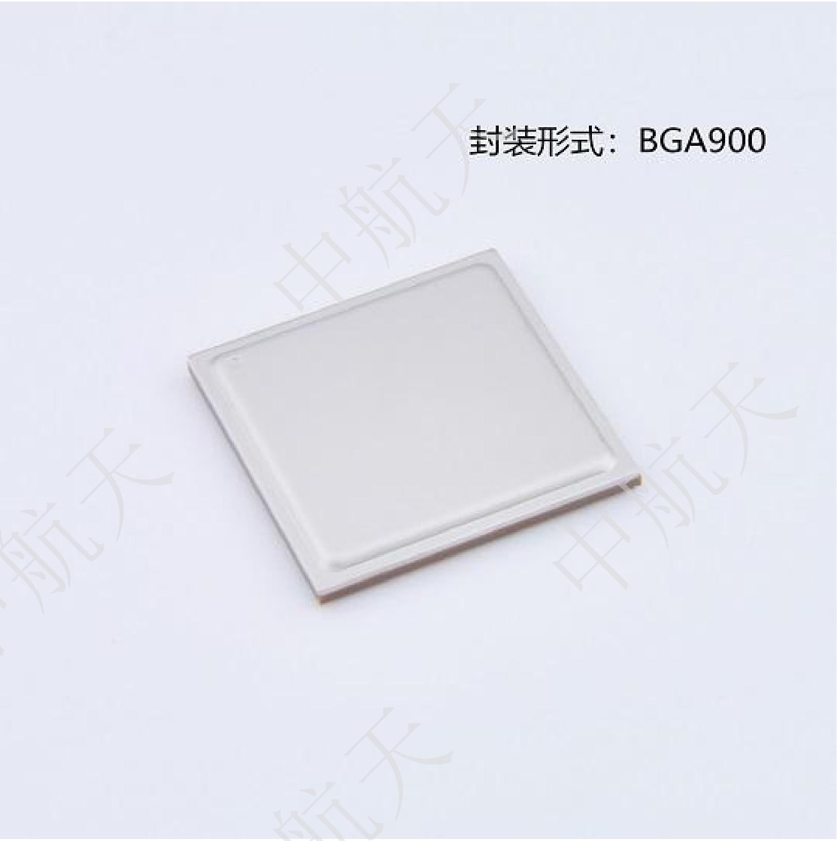
Package:BGA900